

2.0 Common-Emitter Amplifier
OBJECTIVES
GOALS
The objective of this lab is to to familiarize myself with voltage gain and bandwidth. I will also demonstrate how a 2N3904 npn BJT (Bipolar Junction Transistor) can be used to create a Common-Emitter Amplifier (CE Amp).
Chapter 2 Goals
-
Become familiar with gain/bandwidth
-
Become familiar with a CE amplifier
-
Become familiar with LTspice and use it to analyze the CE amplifier circuit
-
Breadboard and test a CE amplifier circuit
2.1 Gain and Bandwidth
Gain and bandwidth are the main components that characterize an amplifier. Typically, most amplifiers exhibit a constant gain over some range of frequency values, also known as the bandwidth (BW). Because frequency is plotted on a log scale, the bandwidth will be observed on a Bode plot and requires voltage gain to be converted to decibels (dB). Specifically, I was looking for a 3-dB drop in the gain to find the 3-dB BW.
A signal generator was used to control the amplitude and frequency of the input voltage amplitude. The output voltage amplitude was measured on the oscilloscope (O-scope) and I used a dual channel O-scope to observe the input and output signals simultaneously due to the varying frequencies observed.
2.2 Common Emitter Amplifier
To build the amplifier, an npn bipolar junction transistor (BJT) was used because the forward-active mode of the BJT is more ideal for amplifier applications. In this mode, the collector current is greater than zero and the total voltage from collector to emitter is slightly greater than half a volt. The relationship between the collector and base currents and the the forward current gain term also makes the 2N3904 BJT that we will be using more ideal because the gain has a broad range of values.
For the DC portion of the circuit, I have to establish the DC operating point, or Q-point, to ensure I design an optimal amplifier . Using the same 4-resistor (4R) biasing network from Digital Electronics, I will stabilize the Q-point against variations in the forward gain term by finding the collector current and DC voltage from the collector to emitter. Using the 4R bias scheme in Figure 1, Exercise 2.1 and Exercise 2.2 will demonstrate how to calculate the Q-point as well as get an idea of what the range will be for the varying forward gain values.
Then, coupling and bypass capacitors are added to the now AC circuit to complete the small signal amplifier. When selecting coupling capacitors, I had to also consider the frequency of operation because the impedance is also dependent upon frequency and a low impedance is needed to avoid a significant drop in the signal across the capacitor. For Exercise 2.3, the impedance is calculated with two different capacitor values to demonstrate which capacitance will give the more ideal impedance value.
Finally, a hybrid-pi AC model is used to replace the BJT and I could analyze the AC equivalent circuit to determine the gain of the CE amplifier. With the same AC circuit and the example in Exercise 2.4 , I can calculate the mid-band gain, transconductance, and resistance.
2.3 LTspice Simulation of the CE Amplifier
Prior to breadboarding the circuit, I created a simulation of the amplifier circuit in LTspice, a circuit simulator package. This lab will also build upon my knowledge of the software from Digital Electronics and serve as a review for building circuits in LTspice. First, the DC portion of the CE amplifier shown in Figure 2 is created and simulated to display the voltages, currents, and power dissipated in Figure 3. Some values to note include: Vb = 1.87535 V, Vc = 5.35731 V, and Ve = 1.16638 V.
Based on the simulation, the resistance values are optimal because the collector current is positive, the voltage from the base to emitter is 0.70897 V, and the voltage from the collector to emitter is a few votes. LTspice also displayed that the total power dissipated by the circuit is 75.097175 mW.
Next, I added the necessary components to create the AC circuit in Figure 4 and observed the transient simulation. The stop time was set to 4 ms for more multiple wavelengths of output and the results are displayed in Figure 5.
With the same AC circuit from Figure 5, the gain of the amplifier was calculated to be 36.684 V/V using the voltage input and output amplitude at no specific point. I also created a Bode plot using the AC Analysis function and the settings displayed in Figure 6 to put the voltage in dB. The equation "20*log(V(vout)/V(vin))" was input at the top of the plot to ensure the amplifier gain was in dB and the results were displayed in Figure 7. Based on my simulated Bode plot, the simulated 3 dB bandwidth for my amplifier is from 1 kHz to 100 kHz.
To enhance my learning of the circuit's functionality, I went through a couple of scenarios making changes and removing components to observe the new output. For the first scenario, I removed the bypass capacitor and re-ran the simulation. The results shown in Figure 8 indicate that the response has a lower gain.
For the next scenario, I returned to Figure 7 and switched the Rb1 and Rb2 resistors. I expected the results to be drastically different due to the difference in value. The results in Figure 9 match my expectations and the response inverted seems to start off high before cutting off.
Then, I rearranged the circuit to look like Figure 7 again before changing the coupling capacitance values to 1 nF. The results shown in Figure 10 show that the bandwidth has decreased significantly and appears inverted.
Finally, I configured the circuit to look like Figure 7 before mirroring the BJT and rerunning the simulation. The results shown in Figure 11 conclude that the transistor is operating in reverse mode.
2.4 Build and Test a Common Emitter Amplifier
For the final section of this lab, I will be assembling the DC and AC circuits mentioned earlier while also reviewing how to breadboard a circuit and use the equipment. Starting with the DC circuit shown in Figure 2, I wired the breadboard correctly before using the Digital Multimeter (DMM) to probe the voltage at my transistor's base, emitter, and collector. I recorded said voltages into Table 1 and ensured that they were close to the same values recorded in the LTspice simulation.
With my transistor meeting all of the requirements, I added the remaining components to create the AC circuit shown in Figure 4. The function generator was configured to output a 1 kHz sine wave with a 10 mV amplitude and the dual mode function was enabled to view the input and output and display the results shown in Figure 12.
Next, I calculated the amplifier voltage gain by dividing the output voltage amplitude by the input voltage amplitude and was expecting the gain to be close to 50 V/V. In addition to calculating the gain for the circuit with a 1 kohm load resistor, I also changed out the load resistance with significantly smaller and larger resistors to observe how load resistance affects the gain. The results were recorded into Table 2 and compared on a plot of gain vs. resistance in Figure 13. From that, it was determined that an audio amplifier using an 8 ohm impedance speaker will not perform well because a very small and very large impedance does not return an ideal voltage gain. An example of the CE amplifier with a different load resistance is shown in Figure 14.
An observation I made when recording the gain for the larger load resistances concerned how high the output's amplitude was getting. For example, the output in Figure 15 is significantly larger at 1.75 V while the input's amplitude remains around 18.8 mV. To calculate the gain, I divided the output amplitude by two to drop the output to half power and then solved for the gain to get the values in Table 3 for the 10 kohm and 100 kohm load resistances.
Finally, I replaced the load resistance with the original 1 kohm before measuring the gain at different frequencies while also keeping the time base in mind. I calculated the gain, converted the value into decibels using the equation 20*log(vout/vin), and recorded the results for each frequency into Table 3 before plotting it on the Bode plot in Figure 16. Using the same Bode plot, it was determined that the bandwidth was from 1 kHz to 300 kHz.
While completing the final step of the lab, I also observed that as I increased the frequency, the output signal's amplitude also increased and appeared significantly larger than the fairly constant input amplitude. This would force a change in the scale and require slight adjustments in amplitudes to maintain consistent values. For example, the signal shown in Figure 17 shows the output signal operating on a higher scale than the input signal. To account for this, I switched between the source channels and recorded that source's amplitude into Table 3 to solve for the gain. Figure 17 shows the output signal as the source while Figure 18 shows the input signal as the source.
I also included a screen capture of the amplified output signal at a higher frequency in Figure 19 to show the difference between the signal at low and high frequencies.

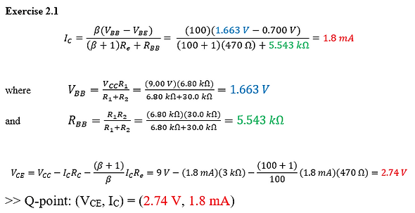
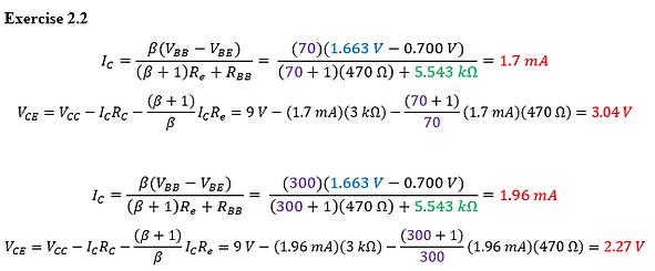
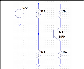
Figure 1: 4R Biasing Network for DC Circuit

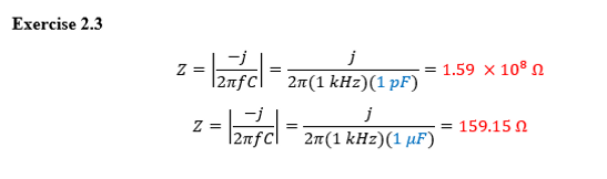

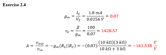


Figure 2: CE Amplifier DC circuit
Figure 3: LTspice Simulation of DC Circuit
Figure 4: CE Amplifier AC Circuit

Figure 5: Transient Results of AC Circuit


Figure 7: Bode Plot of CE Amplifier
Figure 6: Parameters for AC Analysis

Figure 8: CE Amplifier w/o bypass capacitor

Figure 9: CE Amplifier with swapped resistors

Figure 10: CE Amplifier with 1 nF capacitors

Figure 11: CE Amplifier with flipped BJT

Table 1: Operating Parameters

Figure 12: Input and Output of CE Amplifier
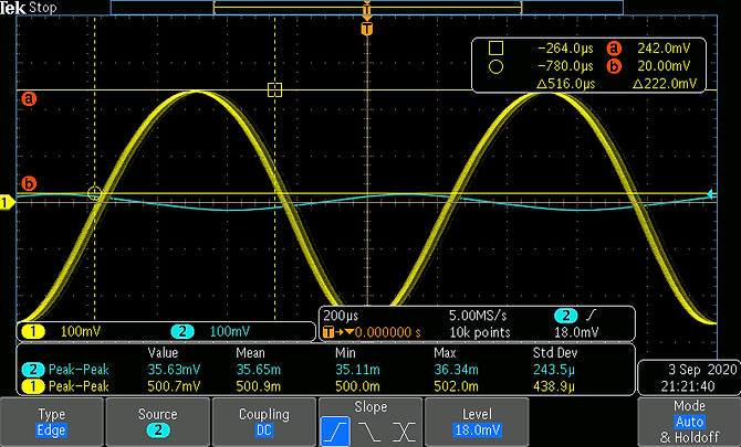

Table 2: Gain with Different Load Resistances
Figure 14: Voltage Input and Output with 100 ohm resistor

Figure 13: Gain vs Resistance Plot
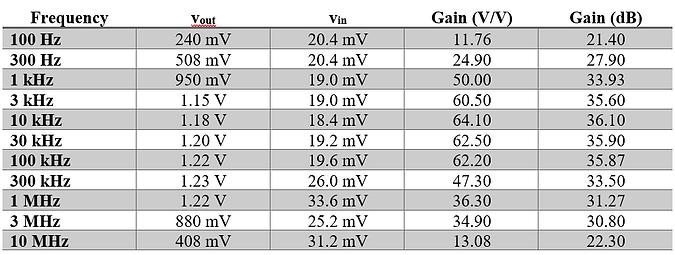
Table 3: Voltage Gain for different Frequencies
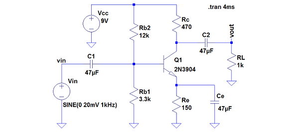

Figure 16: Bode Plot of Gain vs Varying Frequencies
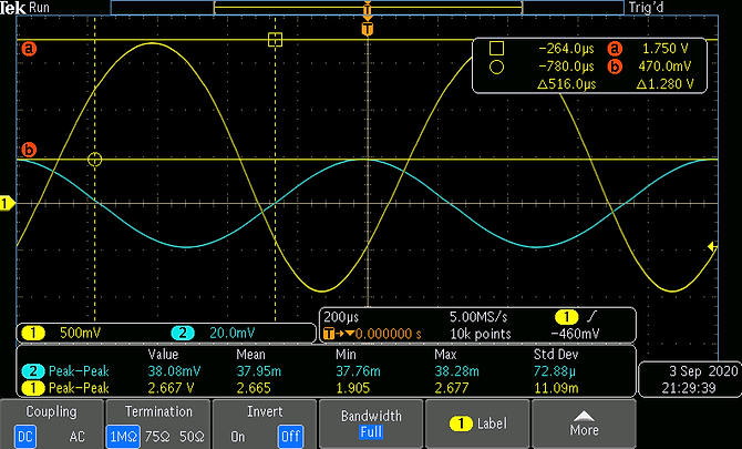
Figure 15: Amplifier with 10 kohm load resistance
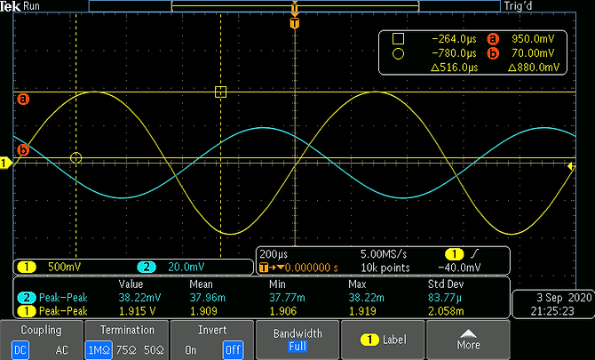
Figure 17: Amplifier at 1kHz with Output as Source

Figure 18: Amplifier at 1kHz with Input as Source

Figure 19: Amplifier at 100 kHz
Reflective Writing
I quickly realized that this lab is a continuance of material learned in Digital Electronics. Within that class, we covered the basics of bipolar junction transistors and 4R biasing networks and how they can be applied to things like amplifiers. It was also a good review for breadboarding circuits. I initially had some trouble with my personal transistor, but having to troubleshoot the circuit and rebuild it from scratch was very helpful considering it allowed me to solve the issue in real-time.