

3.0 Audio Amplifier
OBJECTIVES
GOALS
The objective of this lab is to build on the CE amp created in the previous week and continue constructing an audio amplifier using a transistor level design.
Chapter 3 Goals
-
Become familiar with, analyze, and construct the following amplifiers:
-
Common-collector (CC) amplifier
-
CE-CC two stage amplifier
-
Class AB push-pull amplifier
-
CE-class AB two stage amplifier
-
3.1 Buffer Amplifier
A buffer amplifier is placed between an amplifier and a low resistance load and presents a high input impedance. It can be realized with a Bipolar Junction Transistor (BJT) through a common-collector, or emitter-follower, configuration because the output on the emitter follows the input signal on the base.
3.2 LTspice: Two-Stage BJT Amplifier
Using the LTspice software, the CC amplifier is simulated using the schematic shown in Figure 1. First, the DC Operating Point function of the program was run to determine the Q-point of the 2N3904 NPN transistor by subtracting the the voltage of the emitter from the voltage of the collector. Based on the list of voltages and currents displayed in Figure 2, the Q-point was calculated to be (2.9716 V, 127.7 mA). Then, a transient simulation was run to determine the gain of the same CC amplifier in Figure 1. With an 8 ms stop time, 4 ms delay time, and 1us time step, the gain with a 10 ohm load resistor was 0.9 V/V based on the results shown in Figure 3.
It was also noted that reducing the current through the transistor would reduce the power requirement. To test this theory, the resistor connected to the emitter (Re) is increased from 47 ohms to 100 ohms because resistance is indirectly proportional to current when calculating power. Using the schematic shown in Figure 4, the simulation was re-ran and the Q-point indicated that the Vce value only slightly decreased to 2.232 V, while the current through the collector was a little more than half of the original schematic at 67.423 mA.
Next, a two-stage amplifier circuit, using the CE amplifier from the previous lab and the CC amplifier created at the beginning of this section, was created and simulated using the schematic shown in Figure 5. The amplitude of the voltage source is initially set to 0 V and the DC Operating Point function was run to determine the power dissipated in the circuit. Based on the results shown at the bottom of the screen in Figure 6, the power dissipated is -1.2317588 W. This value represents the quiescent power dissipation and it is negative because of the current polarity of the schematic. When the voltage source amplitude is raised to 10 mV, a transient simulation was run and the results shown in Figure 7 determine that the gain of the amplifier is an ideal 55 V/V.
However, the output can also produce a distorted audio signal because of the range of values it can output. Typically, an output where the positive peak is at a higher amplitude than the negative peak is an example of this distorted signal. For example, the input signal amplitude was increased to 20 mV and re-simulated to get the results shown in Figure 8. The distortion can be observed at the negative peak of the output where it begins to clip.
3.3 Build and Test the Two-Stage Amplifier
To begin building the two-stage amplifier, the speaker was prepared by soldering two wires to the speaker's eyelet and then tested by applying an audio wave through it and observing the input and output. A 1kHz sine wave is created using the function generator and the input signal amplitude is set to 10 mV to keep the distortion minimal. The output was observed on the oscilloscope using the schematic shown in Figure 9 and the initial input voltage was recorded at 2.040 V, as shown in Figure 10. Once the speaker was connected, the input voltage decreased to 276.0 mV and the results can be analyzed in Figure 11. The volume of the speaker began as a moderately low whine and got louder by increasing the input amplitude on the function generator.
Next, the CE amplifier from the previous lab was built using the schematic shown in Figure 12 and inserted between the function generator and the speaker as shown in Figure 13. The function generator will act as the 1 kHz sine wave in the schematic and the 1 kohm load resistor is replaced with the speaker. The output signal is shown in Figure 14 and the sound was similar in volume to the one from the previous section.
Then, the CC amplifier was built using the schematic shown in Figure 1 and inserted between the function generator and the speaker the same way that the CE amplifier was inserted in Figure 13. The function generator will again act as the 1 kHz sine wave and the 10 ohm load resistor is replaced with the speaker. The output signal is shown in Figure 15 and the sound was quieter in volume.
Each amplifier is then added to create the two-stage amplifier shown in the schematic in Figure 16 and inserted between the function generator and the speaker as indicated in Figure 17. The output signal at the speaker is shown in Figure 18 and the thicker line indicates that it was a little noisy. When conducting the sound check, it was determined that the sound was the loudest when compared to the sound checks performed for the CE and CC amplifier connected to the speaker separately.
The speaker was then replaced with a 10 ohm resistor and the input and output were analyzed on the oscilloscope and displayed in Figure 19 and Figure 20 respectively. Both the amplitudes and the gain were recorded in Table 1 below.
The power dissipated was also determined for the two-stage amplifier by disconnecting the input signal directly connected to the circuit and feeding the voltage supply through a 100 ohm resistor as shown in Figure 21. The DC voltage supply was then adjusted to 15.7 V so that 9 V appeared on the other side of the resistor. The voltage drop across the resistor was then divided by the 100 ohm resistance to calculate the current and that answer was multiplied by the Vcc value, 9 V to calculate power dissipated. With the voltage drop being 6.7 V, the current is 67 mA and the power dissipated is 603 mW.
3.4 Class AB Push-Pull Amplifier (LTspice)
A class AB amplifier will solve the distortion problem that occurs because the PN junctions in the BJT's require around 0.7 V to turn on. However it won't have high efficiency without diodes placed in the base bias to ensure a sufficient voltage can turn on the PN junctions. The push-pull configuration of these amplifiers will help create an ideal voltage gain.
First, the default Class B push-pull amplifier was simulated in LTspice using the schematic shown in Figure 22. The amplitude of the voltage source was set to 0 V before the DC Operating Point and Transient simulation were ran to get the results displayed in Figure 23. It was also determined that the quiescent power dissipated was 4.474e-16 W.
The source amplitude was then increased to 2 V and the output is observed using the transient simulation and shown in Figure 24. The average dissipation power was measured to be -297.41 mW and the negative sign indicated that the DC source is providing power.
Next, diodes were added to observe an output with less distortion. Using the schematic shown in Figure 25, the source amplitude was set to 0 V and the DC Operating Point simulation was run to calculate the total power dissipated. The results are shown in Figure 26 and the current was calculated to be 0.09 A while the power dissipated was calculated to be 0.81 W. Compared to the dissipated power found for the Class B push-pull amplifier, the value for the AB push-pull is a lot larger.
Then, the source amplitude is raised to 2 V and the Transient simulation results are shown in Figure 27. The average dissipated power was also determined to be -501.33 mW, as shown in Figure 28. Compared to the value calculated for the Class B push-pull amplifier, the new average power dissipation is almost doubled.
3.4 Class AB Push-Pull Amplifier (Build and Test)
Finally, the Class B push-pull amplifier shown in Figure 22 is tested by first running the voltage supply through a 100 ohm resistor and adjusting the voltage so that 9 V is going into the circuit. A 10 ohm speaker replaced the speaker and the bias voltage with no input signal was calculated to be 9.8 V. Therefore, the current was calculated to be 8 mA and the power dissipated was 72 mA. Once the input amplitude was set to 2 V, the output displayed in Figure 29 looked similar to the results shown in the LTspice simulation in Figure 23.
Then, the Class AB push-pull amplifier shown in Figure 25 is tested using the same process. the 10 ohm speaker is replaced the speaker and the bias voltage with no input signal was calculated to also be 9.8 V. Therefore, the current and power dissipated share the same values with the Class B push-pull amplifier. The input amplitude was set to 2 V and the output displayed in Figure 30 also replicated the results shown in the LTspice simulation in Figure 23 as well as the results from the Figure 29.
Afterwards, the 10 ohm resistor is replaced with the speaker and the clear and stable sound that is produced indicates that this amplifier is sufficient for the radio. Now, this AB push-pull amplifier will replace the second stage CC amplifier between the function generator and the speaker in Figure 17. The gain should then be around 0.8 V/V.
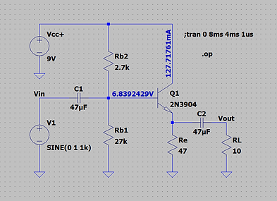

Figure 1: CC Amplifier Schematic
Figure 2: DC Operating Point of CC Amplifier

Figure 3: Transient of CC Amplifier

Figure 4: CC Amplifier with Re = 100 ohm
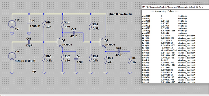
Figure 5: Two-Stage CE-CC Amplifier

Figure 6: Two-Stage Amplifier w/ Power Dissipation

Figure 7: Two-Stage Amplifier Transient with Vs = 10 mV
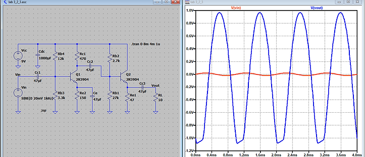
Figure 8: Two-Stage Amplifier Transient w/ Vs = 20 mV

Figure 10: Input without Speaker
Figure 9: Generator to Speaker


Figure 11: Input with Speaker
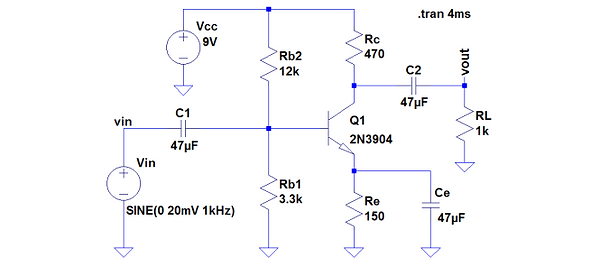
Figure 12: CE Amplifier Schematic

Figure 13: Generator - CE Amplifier - Speaker

Figure 14: Output for CE Amplifier

Figure 15: Output for CC Amplifier
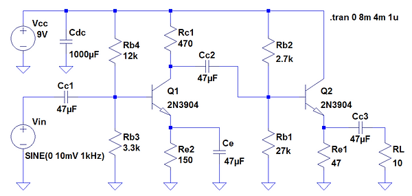
Figure 16: Two-Stage Amplifier Schematic
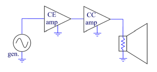
Figure 17: Generator - CE Amplifier - CC Amplifier - Speaker

Figure 18: Output for Two-Stage Amplifier


Figure 19: Two-Stage Amplifier w/o Speaker (Output)
Figure 20: Two-Stage Amplifier w/o Speaker (Input)
Table 1: Gain for Two-Stage Amplifier

Figure 21: Voltage Drop for Power Dissipation

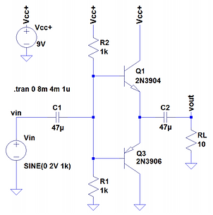
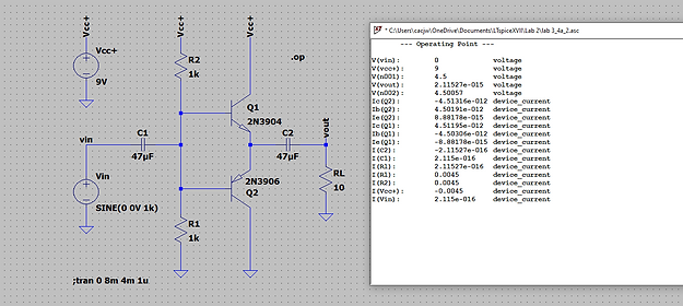
Figure 22: Class B Push-Pull Amplifier Schematic
Figure 23: Class B Push-Pull LTspice Simulation w/ 0 V Input
Figure 25: AB Push-Pull Amplifier Schematic
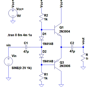
Figure 24: Class B Push-Pull LTspice Simulation w/ 2 V Input

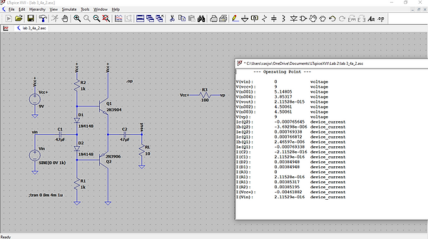
Figure 26: AB Push-Pull in LTspice


Figure 27: AB Push-Pull LTspice Simulation w/ 0 V Input
Figure 28: AB Push-Pull LTspice Simulation w/ 0 V Input

Figure 29: Output for B Push-Pull Amplifier

Figure 30: Output for AB Push-Pull Amplifier
Reflective Writing
Initially, constructing the CE and CC amplifiers went smoothly and the outputs were close to ideal. However, constructing the two-stage amplifier proved to be more difficult. Considering this lab forced ~90% of the class to come back in to finish makes me think that this lab should probably be broken down further. My two-stage amplifier was drawing a large amount of current through the transistor after rebuilding it alongside my TA 3 times. I'm honestly still not sure what the problem was, but I was able to look over my TA's circuit and understand what was supposed to happen.